
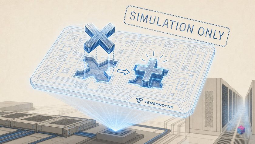
A US-German startup says it can beat Nvidia at inference by doing the one thing chip designers usually avoid: throwing away the multiplier. The bet is mathematical, the silicon is unbuilt, and every headline number comes from simulation.
What Tensordyne's Napier chip actually does
Napier is a 3nm AI inference chip built around a logarithmic number system that turns matrix multiplications into additions. Announced by Tensordyne on June 15, 2026 , the chip exploits the identity log(A×B) = log(A) + log(B): in log space, a multiply becomes an add, and adders need far less die area than multipliers at equivalent precision .
Per ServeTheHome, the die packs 138 billion transistors on TSMC's 3nm process, 256 MB of on-chip SRAM (claimed ~5× Nvidia's Blackwell), and 144 GB of HBM3E, clocking its accelerator core at 1.33 GHz inside a ~300W envelope . The extra SRAM is the point: freeing multiplier area lets Tensordyne rebalance toward memory.
The flagship system is the TDN72 pod: 72 accelerators per rack, drawing ~120 kW yet remaining air-cooled, with ~68 petaflops aggregate compute and ~42 TB of HBM . Chips link over a proprietary TDN Link interconnect rated at ~1 TB/s with sub-microsecond latency .
One caveat frames everything below: Napier has only taped out. No shipping silicon exists, and every cited efficiency ratio originates from Tensordyne's own simulations .
Why log arithmetic frees up die area
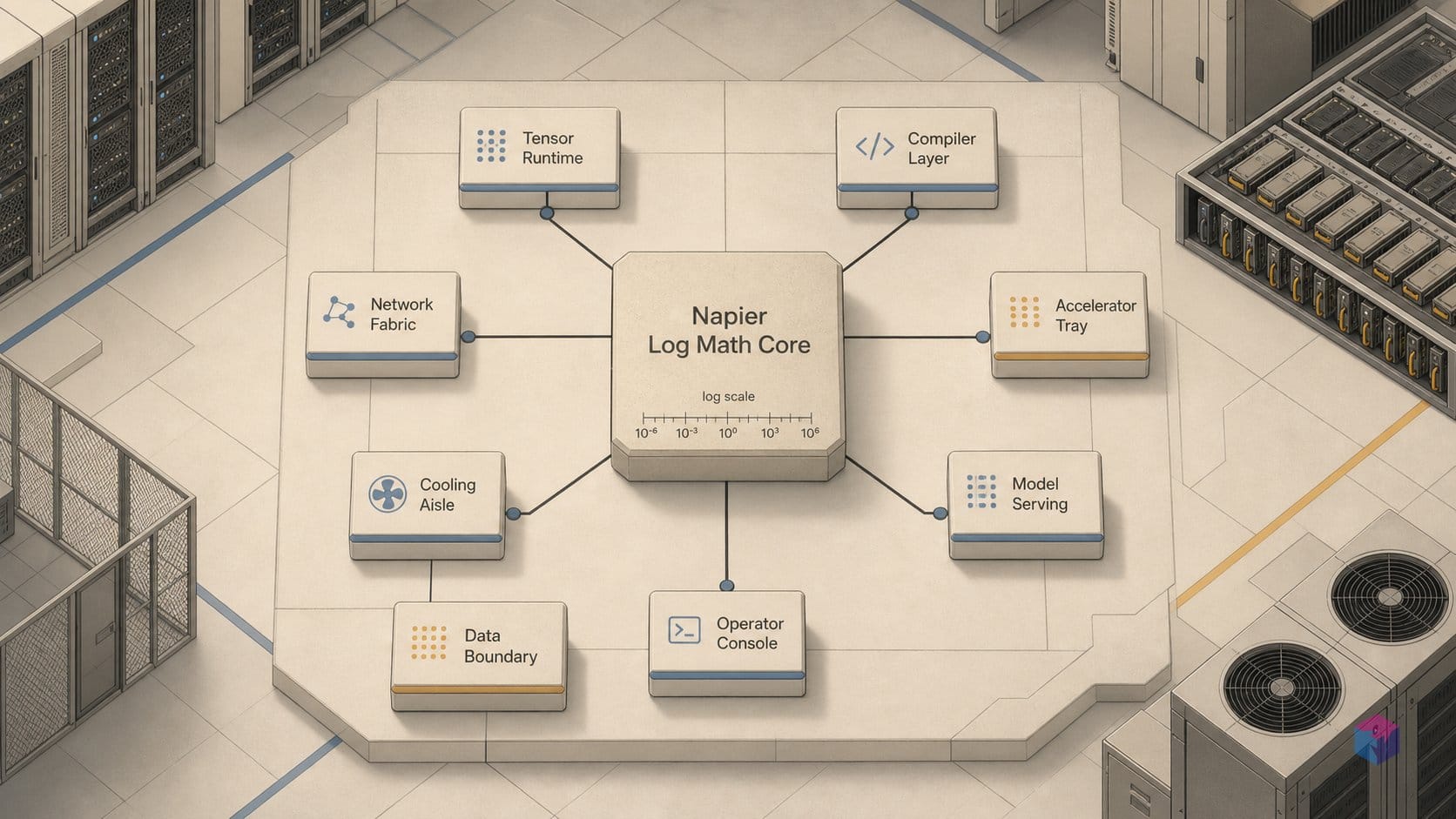
The area savings come from a substitution at the gate level: an adder occupies far less silicon than a multiplier of equivalent precision. Because log(A × B) = log(A) + log(B), working in log space converts matrix multiplications into additions, and Tensordyne redeployed the reclaimed area to memory. Napier carries 256 MB of on-chip SRAM , roughly five times the on-chip SRAM the company attributes to Nvidia's Blackwell .
The arithmetic itself has a credible academic track record. Miyashita, Lee, and Murmann showed in 2016 that weights and activations could be encoded down to 3 bits with negligible classification loss, with log-domain dot products eliminating bulky digital multipliers . The later LNS-Madam work estimated energy reductions of over 90% versus FP32 training while keeping accuracy comparable to full precision .
So why has LNS stayed academic? The historical barrier was always the same: converting between linear floating-point and logarithmic representations consumed the area and energy the arithmetic saved, making LNS a wash in practice. IEEE Spectrum put it bluntly: conversion "took too much time and energy and introduced too many inaccuracies" .
That makes the conversion the entire thesis. VP of AI Gilles Backhus claims the gap is closed:
"No one has figured out how to do the linear to logarithm and logarithm to linear conversion as we have," said Gilles Backhus, VP of AI at Tensordyne (source: IEEE Spectrum).
It is also the part with zero published evidence. No precision metrics, error bounds, or third-party verification of the conversion method exist yet. The claim rests on simulation alone.
TDN72 pod: what the 52U rack contains
The TDN72 is Tensordyne's flagship rack-scale system: 72 Napier accelerators packaged into a single standard 52RU rack drawing roughly 120 kW, and, unusually for this density, air-cooled, with no liquid cooling required . That is the headline structural claim, and the one most worth scrutinizing once hardware ships.
The packaging stacks predictably. Nine Napier chips sit on each 1RU tray (1.3 TB HBM3E per tray), four trays form a pod, and four pods fill the rack: 9 × 4 × 4 = 72 accelerators, ~42 TB of HBM3E aggregate .
| Unit | Contents | HBM3E |
|---|---|---|
| 1RU tray | 9 Napier chips | 1.3 TB |
| Pod | 4 trays (36 chips) | ~5.2 TB |
| 52U rack | 4 pods (72 chips) | ~42 TB |
The rack-level comparison Tensordyne cites: for a 2-trillion-parameter mixture-of-experts model, one 120 kW TDN72 reportedly matches ~9 Nvidia/Groq racks at 1.5 MW . Treat that as simulation, not measurement.
The supplier and traction picture is more concrete:
- Silicon and packaging IP: Broadcom; chassis and networking: HPE and Juniper Networks .
- Named early customers: Cirrascale Cloud Services and BlueSky Compute .
- Leadership: CEO Marc Bolitho, CPO R.K. Anand, with former Starbucks CEO Kevin Johnson on the board .
- Traction: 12+ letters of intent representing $200M+ in forecast demand; a Series D is anticipated in H2 2026 .
Dissecting the 13×/17× efficiency projection
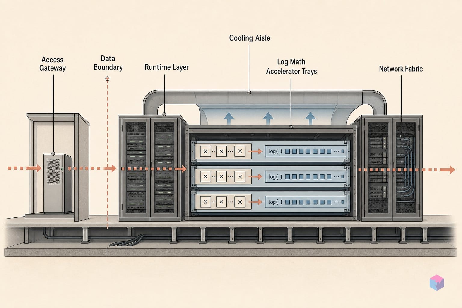
The headline numbers are the reason anyone is paying attention. Tensordyne says a single TDN72 rack delivers 13× higher token throughput and 17× more tokens per watt than Nvidia's GB300 NVL72, while sustaining over 1,000 tokens/second per user. Every one of those figures comes from Tensordyne's own simulations. There is no MLPerf submission and no independent lab measurement as of June 2026.
The economic framing is just as aggressive. IEEE Spectrum cites roughly $11 per million tokens at 1,300 tokens/sec/user, and about 4× faster inference at one-fifth the power versus the GB300. Tensordyne pairs that with a claimed $33M in additional annual revenue potential per rack over an NVL72.
These are plausible if the linear-to-log conversion preserves model accuracy at scale, and unverifiable until it does not. Two caveats from the coverage itself matter here:
- IEEE Spectrum concedes its report "lacks skeptical expert commentary" and that all cited figures rest on simulation.
- ServeTheHome flags untested accuracy and immature software versus CUDA as the primary risks.
| Claim | Figure | Basis |
|---|---|---|
| Token throughput vs GB300 | 13× | Simulation |
| Tokens/watt vs GB300 | 17× | Simulation |
| Cost at 1,300 tok/s/user | ~$11/M tokens | Simulation |
| Revenue uplift per rack | ~$33M/yr | Vendor model |
One thing the magnitude does buy: margin for error. The 17× is large enough that even a 50% miss on real silicon would still be a meaningful efficiency gain. But that math only holds if precision survives. A quality degradation at scale would not shave the multiplier; it would invalidate the comparison entirely.
Log-domain summation error: what the LNS literature warned about
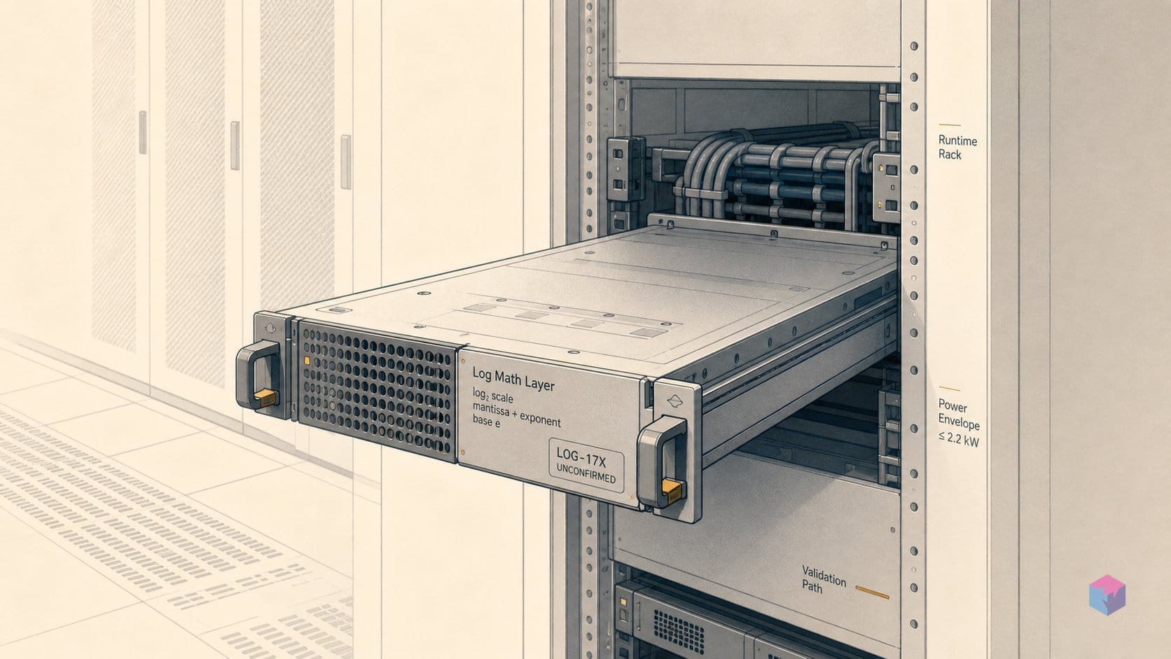
Precision is exactly where logarithmic number systems get hard. Multiplication in log space is closed and exact (log(A × B) = log(A) + log(B)), which is the whole appeal. Addition and subtraction are not. There is no clean log-domain identity for A + B, so every accumulation step must be approximated with look-up tables or piecewise functions, and each approximation injects error. In a transformer doing trillions of summations per token, that error has to stay bounded or model quality drifts.
The academic record is explicit about the tradeoff. Work on low-precision LNS in ACM TACO found that the choice of logarithm base materially affects low-precision error, die area, and power; no single base is globally optimal across workloads. Tune for one, regress on another.
Jeff Johnson's ARITH-2020 paper names the historical failure mode directly: classic LNS saw limited adoption because the summation tables needed for log-domain addition impose high area and power overhead. His dual-base approximate design reports 2.3× and 4.6× better energy efficiency than float32 and float64 vector inner products in 7nm CMOS, gains that exist precisely because the summation cost was attacked head-on.
"No one has figured out how to do the linear to logarithm and logarithm to linear conversion as we have," said Gilles Backhus, VP of AI at Tensordyne (source: IEEE Spectrum).
That is the claim the literature says is hard, and it is the claim with the least evidence. As of June 2026 Tensordyne has published zero precision or error-budget metrics, and no third-party fidelity audit of log-converted weights or activations exists . Until someone measures accuracy on real silicon, the conversion breakthrough is asserted, not demonstrated.
MLPerf fidelity audits: what to demand from Napier in 2027
The earliest a developer can independently test that claim is roughly six months out. Tensordyne's roadmap puts a development and beta cloud at the end of 2026, beta programs in Q1 2027, and production shipments by the end of Q2 2027 . Until then, every number is simulation.
When silicon ships, the minimum credible evidence is concrete and measurable:
- MLPerf Inference submissions on shipping Napier hardware, not vendor simulations, so the 13×/17× projections face a standardized, third-party harness .
- Published log↔linear conversion error budgets at FP8-equivalent and INT8-equivalent precision, the metric the LNS literature flags as the real risk and the one Tensordyne has not disclosed.
- Compiler and framework readiness: there is still no detail on PyTorch or JAX integration, quantization tooling, or how FP8/INT8-trained models map onto the log format without retraining.
Software maturity may decide this faster than peak throughput. As ServeTheHome noted, "the gap between a compelling launch and a successful AI platform is large" . Cluster scheduling, failover semantics, and driver stability are unaddressed, and for production deployments they matter more than tokens per watt.
The takeaway: Napier is a differentiated, well-partnered bet, but treat it as a 2027 question. Demand MLPerf numbers on real silicon and a published accuracy budget before assuming the log-math advantage survives contact with production workloads.
Frequently asked questions
What is the logarithmic number system (LNS) and why does it matter for AI chips?
LNS stores each value as its logarithm. Because log(A × B) = log(A) + log(B), multiplications collapse into additions, and adders occupy less silicon and burn less energy than multipliers, freeing die area for SRAM or other logic. The idea is decades old; Miyashita, Lee, and Murmann showed log-encoded weights down to 3 bits with negligible accuracy loss back in 2016 . It stayed impractical because linear↔log conversion overhead ate the savings. Tensordyne claims a cheap, accurate conversion method ; that claim is currently unverified.
How does Napier's on-chip SRAM compare to Nvidia Blackwell?
Tensordyne reports 256 MB of on-chip SRAM per Napier package, roughly five times the ~51 MB on Nvidia's Blackwell B200 . The extra capacity comes from die area freed by swapping multiplier arrays for adder arrays. More on-chip SRAM means fewer trips to slower off-chip HBM3E during long-context inference, which is where Napier's memory-heavy rebalancing is meant to pay off.
Are the 13×/17× throughput and efficiency numbers independently verified?
No. As of June 2026, the claimed 13× token throughput and 17× tokens per watt versus Nvidia's GB300 NVL72 rest entirely on Tensordyne's own simulations against projected hardware . No MLPerf submission exists, no independent lab has benchmarked the chip, and no shipping silicon is available. IEEE Spectrum notes the launch coverage "lacks skeptical expert commentary" . Earliest independent access is beta in Q1 2027.
What is the core technical risk with LNS arithmetic for neural networks?
Log-domain addition is not closed; it has to be approximated, and that approximation error can accumulate across the hundreds of layers in a transformer. The LNS base also affects precision, area, and power with no single optimal choice . Tensordyne has published no model-accuracy or error-budget metrics on LNS-converted weights, so whether quality survives at scale remains the central open question.
When can engineers actually run workloads on Napier?
Not yet. The chip has only taped out. Tensordyne's roadmap targets a developer/beta cloud by end of 2026, formal beta programs in Q1 2027, and production shipments by end of Q2 2027 . Separately, compiler and framework support (PyTorch, JAX, and quantization tooling that would let models map onto the log format) has not been detailed publicly, and that software readiness is a distinct hurdle from silicon availability.